- 您现在的位置:买卖IC网 > Sheet目录368 > UPD44646363AF5-E22-FQ1-A (Renesas Electronics America)SRAM DDRII 72MBIT 165-PBGA
μ PD44646092A-A, 44646182A-A, 44646362A-A, 44646093A-A, 44646183A-A, 44646363A-A
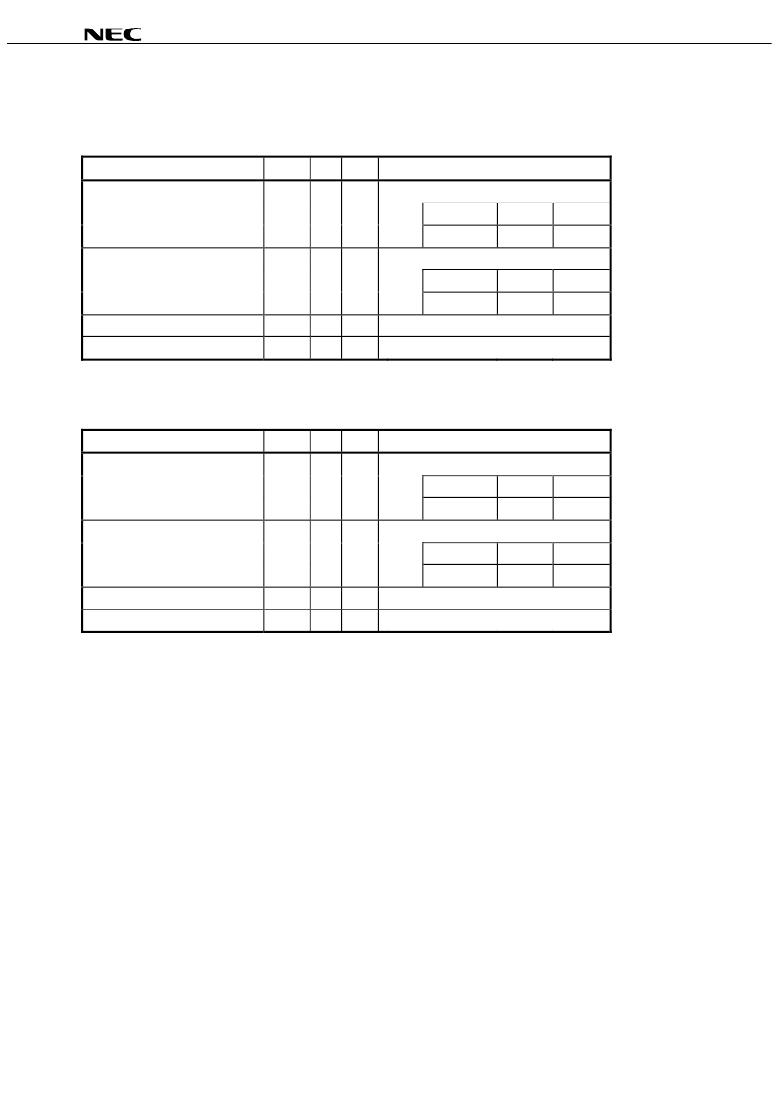
Truth Table
2.0 Clock Cycles Read Latency
[ μ PD44646092A-A], [ μ PD44646182A-A], [ μ PD44646362A-A]
Operation
WRITE cycle
Load address, input write data on
consecutive K and K# rising edge
READ cycle
Load address, read data on
consecutive K and K# rising edge
NOP (No operation)
Clock stop
CLK
L → H
L → H
L → H
Stopped
LD#
L
L
H
X
R,W#
L
H
X
X
DQ
Data in
Input data
Input clock
Data out
Output data
Output clock
DQ = High-Z
Previous state
D A (A+0)
K(t+1) ↑
Q A (A+0)
K(t+2) ↑
D A (A+1)
K#(t+1) ↑
Q A (A+1)
K#(t+2) ↑
2.5 Clock Cycles Read Latency
[ μ PD44646093A-A], [ μ PD44646183A-A], [ μ PD44646363A-A]
Operation
WRITE cycle
Load address, input write data on
consecutive K and K# rising edge
READ cycle
Load address, read data on
consecutive K and K# rising edge
NOP (No operation)
Clock stop
CLK
L → H
L → H
L → H
Stopped
LD#
L
L
H
X
R,W#
L
H
X
X
DQ
Data in
Input data
Input clock
Data out
Output data
Output clock
DQ = High-Z
Previous state
D A (A+0)
K(t+1) ↑
Q A (A+0)
K#(t+2) ↑
D A (A+1)
K#(t+1) ↑
Q A (A+1)
K(t+3) ↑
Remarks
Remarks listed below are for both products with 2.0 and 2.5 Clock Cycles Read Latency.
1. H : HIGH, L : LOW, × : don’t care, ↑ : rising edge.
2. Data inputs are registered at K and K# rising edges. Data outputs are delivered at K and K# rising edges.
3. All control inputs in the truth table must meet setup/hold times around the rising edge (LOW to HIGH) of
K. All control inputs are registered during the rising edge of K.
4. This device contains circuitry that ensure the outputs to be in high impedance during power-up.
5. Refer to state diagram and timing diagrams for clarification.
6. A+0 refers to the address input during a WRITE or READ cycle.
A+1 refers to the next internal burst address in accordance with the burst sequence.
7. It is recommended that K = K# when clock is stopped. This is not essential but permits most rapid restart
by overcoming transmission line charging symmetrically.
Data Sheet M19960EJ2V0DS
11
发布紧急采购,3分钟左右您将得到回复。
相关PDF资料
UPD44647366AF5-E22-FQ1-A
SRAM QDRII 72MBIT 165-PBGA
USB-100
KIT STARTER FOR USB
USBMLCF
USB BDM INTERFACE MC P&E
USBMLPPCBDM
MULTILINK P&E POWERPC USB
V-9767-L
DOOR ECONOGLAS 19" LOCKING
VC-9931
CABINT VISNCB 20.54X23.62X23.62"
VC-9934B
VISIONCAB B 35.40X23.62X23.62"
VLA500-01
IC IGBT GATE DVR/DC-DC CONV 12A
相关代理商/技术参数
UPD44646363AF5-E25-FQ1
功能描述:SRAM DDRII 72MBIT 165-PBGA RoHS:是 类别:集成电路 (IC) >> 存储器 系列:- 标准包装:3,000 系列:- 格式 - 存储器:EEPROMs - 串行 存储器类型:EEPROM 存储容量:8K (1K x 8) 速度:400kHz 接口:I²C,2 线串口 电源电压:1.7 V ~ 5.5 V 工作温度:-40°C ~ 85°C 封装/外壳:8-SOIC(0.154",3.90mm 宽) 供应商设备封装:8-SOIC 包装:带卷 (TR)
UPD44646363AF5-E25-FQ1-A
功能描述:SRAM DDRII 72MBIT 165-PBGA RoHS:是 类别:集成电路 (IC) >> 存储器 系列:- 标准包装:3,000 系列:- 格式 - 存储器:EEPROMs - 串行 存储器类型:EEPROM 存储容量:8K (1K x 8) 速度:400kHz 接口:I²C,2 线串口 电源电压:1.7 V ~ 5.5 V 工作温度:-40°C ~ 85°C 封装/外壳:8-SOIC(0.154",3.90mm 宽) 供应商设备封装:8-SOIC 包装:带卷 (TR)
UPD44647186AF5-E22-FQ1
功能描述:SRAM QDRII 72MBIT 165-PBGA RoHS:是 类别:集成电路 (IC) >> 存储器 系列:- 标准包装:1,000 系列:- 格式 - 存储器:RAM 存储器类型:SRAM - 双端口,同步 存储容量:1.125M(32K x 36) 速度:5ns 接口:并联 电源电压:3.15 V ~ 3.45 V 工作温度:-40°C ~ 85°C 封装/外壳:256-LBGA 供应商设备封装:256-CABGA(17x17) 包装:带卷 (TR) 其它名称:70V3579S5BCI8
UPD44647186AF5-E22-FQ1-A
功能描述:SRAM QDRII 72MBIT 165-PBGA RoHS:是 类别:集成电路 (IC) >> 存储器 系列:- 标准包装:3,000 系列:- 格式 - 存储器:EEPROMs - 串行 存储器类型:EEPROM 存储容量:8K (1K x 8) 速度:400kHz 接口:I²C,2 线串口 电源电压:1.7 V ~ 5.5 V 工作温度:-40°C ~ 85°C 封装/外壳:8-SOIC(0.154",3.90mm 宽) 供应商设备封装:8-SOIC 包装:带卷 (TR)
UPD44647186AF5-E25-FQ1
功能描述:SRAM QDRII 72MBIT 165-PBGA RoHS:是 类别:集成电路 (IC) >> 存储器 系列:- 标准包装:3,000 系列:- 格式 - 存储器:EEPROMs - 串行 存储器类型:EEPROM 存储容量:8K (1K x 8) 速度:400kHz 接口:I²C,2 线串口 电源电压:1.7 V ~ 5.5 V 工作温度:-40°C ~ 85°C 封装/外壳:8-SOIC(0.154",3.90mm 宽) 供应商设备封装:8-SOIC 包装:带卷 (TR)
UPD44647186AF5-E25-FQ1-A
功能描述:SRAM QDRII 72MBIT 165-PBGA RoHS:是 类别:集成电路 (IC) >> 存储器 系列:- 标准包装:3,000 系列:- 格式 - 存储器:EEPROMs - 串行 存储器类型:EEPROM 存储容量:8K (1K x 8) 速度:400kHz 接口:I²C,2 线串口 电源电压:1.7 V ~ 5.5 V 工作温度:-40°C ~ 85°C 封装/外壳:8-SOIC(0.154",3.90mm 宽) 供应商设备封装:8-SOIC 包装:带卷 (TR)
UPD44647366AF5-E22-FQ1
功能描述:SRAM QDRII 72MBIT 165-PBGA RoHS:是 类别:集成电路 (IC) >> 存储器 系列:- 标准包装:3,000 系列:- 格式 - 存储器:EEPROMs - 串行 存储器类型:EEPROM 存储容量:8K (1K x 8) 速度:400kHz 接口:I²C,2 线串口 电源电压:1.7 V ~ 5.5 V 工作温度:-40°C ~ 85°C 封装/外壳:8-SOIC(0.154",3.90mm 宽) 供应商设备封装:8-SOIC 包装:带卷 (TR)
UPD44647366AF5-E22-FQ1-A
功能描述:SRAM QDRII 72MBIT 165-PBGA RoHS:是 类别:集成电路 (IC) >> 存储器 系列:- 标准包装:3,000 系列:- 格式 - 存储器:EEPROMs - 串行 存储器类型:EEPROM 存储容量:8K (1K x 8) 速度:400kHz 接口:I²C,2 线串口 电源电压:1.7 V ~ 5.5 V 工作温度:-40°C ~ 85°C 封装/外壳:8-SOIC(0.154",3.90mm 宽) 供应商设备封装:8-SOIC 包装:带卷 (TR)
